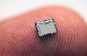
 The small silver square in the picture to the right is a computer chip. It is tiny, just a couple of millimeters across. This chip was made in 1974. It is very early chip technology. By today’s standards the features on the chip are huge. This chip is a memory chip made by RCA. You can see a matrix of dots. Each of these dots is a memory cell. The matrix of cells is 16 across by 8 down. This chip could store 256 bits of information. It was one of first, if not the first, CMOS technology memory chips made. Today chips of this size can store around 1 billion bits of information.
I use the term computer chip, but it is not really a formal term. I use it to differentiate from other types of chips. The first chips were created with a single transistor. Later we learned to create multiple electronic components on a single chip, these are called integrated circuits. Transistors, and integrated circuits, can be analog or digital, or both. Analog applications are things like amplifying an electric signal and cutting off certain frequencies of signals. Digital applications, which we associate with computers, deal with binary signals. So, I could use the term digital chips, but there are many digital chips that would never see the inside of a computer. Now as it turns out, I collect all of the above, but computer chips are the hottest collectible.
Very few people have seen chips. You generally see the package that holds them. Chips can’t be used in computers, or any other electric equipment, until it is put in a package that can interface with circuit boards and computers. Packages are things that we see when we look in computers and on circuit boards. Chips are like the brain, and packages are like the skull. 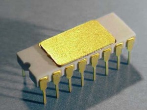 The package to the left is called a Dual In-line Package, or DIP for short. This particular DIP has a body made of white ceramic. The sixteen external leads around the body are made of an alloy called Kevar and coated with gold. The lid on top is made of the same metals. Under the lid is a cavity where the chip would be glued with gold epoxy. The chip would connected with gold interconnect wires to connect the chip to the external leads.
Packages are amazing engineering devices in their own right. The package had to be made with wires imbedded in the ceramic to connect the chip with the external leads. The side of the body had pads where the external leads would be brazed. The hot and cold expansion characteristics of the body and all metal parts, and the chip, all need to be the same to avoid cracking and breaking in a variety of temperatures. The chip would be installed in the air-tight package in a nitrogen atmosphere to keep the chip from oxidizing. Most chip failures were related to package failures.
To see the details of a computer chip, you need a microscope. Below are some extreme closeups of the chip in the picture at top of the page. Click on the pictures to see large versions of the images.
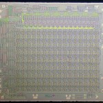 This is a view of the entire chip under This is a view of the entire chip undera microscope at 25x magnification |
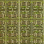 This is a 125x magnification of the This is a 125x magnification of thememory cells |
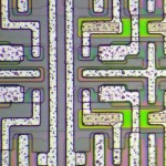 This is a 575x magnification of a single This is a 575x magnification of a singlememory cell |
To learn more about how computer chips are made: Click Here
